

RayRailSwSense
Hardware
BTH-based high-side DC rail switch with current/diagnostic sense and switched-output voltage sensing for amplifier and instrumentation development. The historical BTH50030 assembly was tested; builders must verify operating limits and controller interfaces.
Overview
RayRailSwSense is an open-hardware Public Engineering Reference — AS-IS under the CERN-OHL-P v2.0 hardware license. The published BTH redesign includes editable KiCad sources, a tested-population BOM, manufacturing files and integration, assembly, history and limitations documentation. Parent-controller firmware is not included.
PCBWay fabricated the BTH board; RF StateSide hand-populated and reflow-assembled it, then successfully tested it with RayPowerMeter and RaySspaController. That historical integration does not establish a universal connector interface or a complete validated voltage/current operating envelope.
The prepared P2-prep-01 manufacturing package has not itself been refabricated or physically tested. Historical hardware results are not physical acceptance of the regenerated outputs. The project is Dormant: available as an engineering reference, not currently under active development, and may be revisited. No commercial certification or guaranteed performance is claimed.
At a Glance
- • Tested population: BTH500301LUAAUMA1
- • R4 = 2 kΩ; calculated nominal sense scaling
- • Six-position J3 carries rail and controller signals
- • Fuse holder, TVS and ferrite bead are design features
- • ADC protection and verified interface required
Key Features
Smart High-Side Switching
- U1: historically tested BTH500301LUAAUMA1
- Switch control through J3-4 to IN; DEN supplied from the local 3.3 V network
- Device protection behavior is conditional; verify the installed device requirements
- Off state is not safety isolation; no universal reverse-polarity or surge guarantee
Current Sense for Telemetry
- IS carries load-current and diagnostic information
- Calculated nominal 58.8 mV/A with R4 = 2 kΩ; calibrate each system
- Fault-state output can exceed ADC range; protection is external
- J3-2 senses divided switched Vout, not unswitched input voltage
Protection & Filtering Components
- F1 fuse holder and removable automotive-type fuse are separate parts
- SMCJ85A TVS present; not coordinated protection for the complete board
- Voltage-divider and current/diagnostic filter networks
- Murata BLM31PG121SN1L on the external 3.3 V feed
Open Integration
- External controller must respect device timing, voltage and fault requirements
- J3 carries raw Vout, divided Vout, external 3.3 V, control, sense and ground
- No onboard 3.3 V regulator or controller logic
- Do not assume straight-through RaySspaController connector compatibility
Hardware Overview
J1 is the DC input; F1 feeds U1's supply tab (pad 9). U1 pins 5–8 feed J2, the switched output. Ground is common; this is not a galvanically isolated switch or measurement interface. The individual PCB is 60 × 40 mm.
| Population | Evidence | Calculated nominal sense slope, R4 = 2 kΩ |
|---|---|---|
| BTH500301LUAAUMA1 | Historical fabricated/tested assembly | 58.8 mV/A (typical differential ratio 34,000) |
| BTH500151LUAAUMA1 | Unverified alternative; different device characteristics, not a higher-rated board | 38.5 mV/A (typical differential ratio 52,000) |
The owner-confirmed tested population used R4 = 2 kΩ, Murata BLM31PG121SN1L and a 25 A / 32 V automotive-type fuse. Its fuse marking does not establish continuous board-current capability. FB1 is a 1206 component fitted on retained 0805-designated lands; check seating and solder joints.
Sense slopes are calculations before device offset and receiver loading, not measured calibration or guaranteed accuracy. Device/resistor tolerances, temperature and the receiving ADC path require system calibration. The alternative population requires engineering review and independent testing.
J3 — Six-Position System Interface
| Pin | Function | Circuit / integration requirement |
|---|---|---|
| 1 | Raw switched Vout | Direct J2 connection; can carry the switched rail voltage, not a logic or ADC-level signal |
| 2 | Divided Vout | R5 = 82 kΩ / R6 = 4.7 kΩ; nominal Vout × 4.7/(82 + 4.7) for a high-impedance receiver |
| 3 | External 3.3 V input | FB1 feeds the local rail and R2 = 4.7 kΩ to DEN; not an onboard regulated output |
| 4 | Switch control | R1 = 4.7 kΩ to U1 IN, active high; respect the installed device's electrical/timing requirements |
| 5 | Current/diagnostic sense | IS/R4 node through R3 = 4.7 kΩ; C2 = 10 nF to ground; fault voltage can exceed ADC limits |
| 6 | Ground | Measurement and logic return |
DEN is fed from the local external 3.3 V network, not independently exposed as a J3 control. Check connector orientation against KiCad pad numbers and verify host IN/DEN timing and fault reset.
J3-5 is not a guaranteed 3.3 V ADC-safe output. The BTH50030 datasheet fault current can reach 5.2 mA under its stated conditions; across 2 kΩ this corresponds to a calculated 10.4 V before compliance/loading effects. R3 limits current but does not clamp voltage. The receiver needs appropriate protection, clamping/scaling and diagnostic fault handling.
Operating Limits Must Be Established for the Installation
The installed Littelfuse 178.6165.0002 holder has manufacturer component limits of 32 VDC maximum, 30 A maximum and a 22.5 A continuous component figure for its four-pin-per-terminal construction. Do not exceed the holder's limits or treat its maximum current as continuous.
These component limits and the historical fuse value do not establish a complete-board voltage/current rating. Establish the usable envelope from the switch, PCB, fuse/holder, contacts, wiring, thermal conditions and external system requirements. Historical test voltage, sustained current, duration and temperature are not established by the retained evidence.
The SMCJ85A TVS's 85 V standoff and stated 137 V pulse clamping do not coordinate protection for U1's 70 V absolute supply maximum or C1's 50 V component rating. Those values are component boundaries, not operating recommendations. No guaranteed surge, overcurrent, fault-survival, thermal capability or measurement accuracy is claimed.
Controller Integration
Do not assume straight-through connector compatibility. Saved RaySspaController J4–J7 revisions assign pin 1 to voltage sense and pin 2 to +12 V; RayRailSwSense J3 uses raw Vout and divided Vout at those positions. Do not connect a straight-through six-wire cable.
Use a verified adapter/interface for the exact controller revision, with appropriate receiver protection, scaling, grounding and signal assignments. Historical successful RaySspaController and RayPowerMeter integration is system evidence, not universal cable compatibility or a qualified operating envelope. The published integration guide's candidate mapping is not a reconstruction of the historical tested harness.
Development History & Prepared Revision
An earlier LTC7001/INA240 design was fabricated and populated. Its original Q1 footprint reversed pins 1 and 5; Q1 was reinstalled in the opposite orientation, and the assembled board was successfully tested with RaySspaController. That separate historical design is not the build source for this release.
The later BTH redesign was fabricated by PCBWay, hand-populated and reflow-assembled, then tested with RayPowerMeter and RaySspaController using the confirmed BTH50030 population.
P2-prep-01 preserves copper, pads, drilling, routing and placement while reconciling population records, local libraries and fabrication metadata. Revised labeling and generated outputs distinguish it from the original submission; this exact package has not itself been refabricated or physically tested. Review known limitations, retained ERC findings and fabricator CAM requirements before manufacture. No support, certification or continued development is promised.
Gallery
Current P2-prep-01 PCB Front
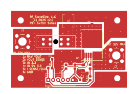
Current PCB-front KiCad export from the public reference. This is a CAD view, not physical validation of P2-prep-01. The earlier 3D render is retained in the media archive; its printed operating labels are superseded.
RayRailSwSense Assembled Board
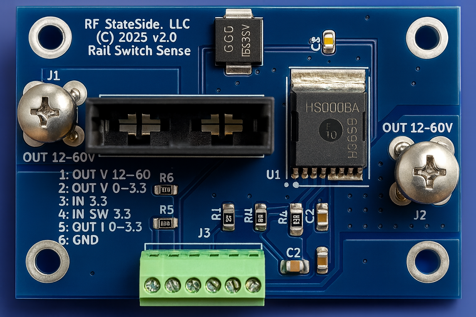
Historical fabricated RayRailSwSense BTH board. Original RF StateSide photograph; AI used only for cropping and cleanup. Historical printed rail/sense labels are not released operating ratings or ADC limits. This photograph does not validate the prepared P2-prep-01 package.
Published BTH Schematic
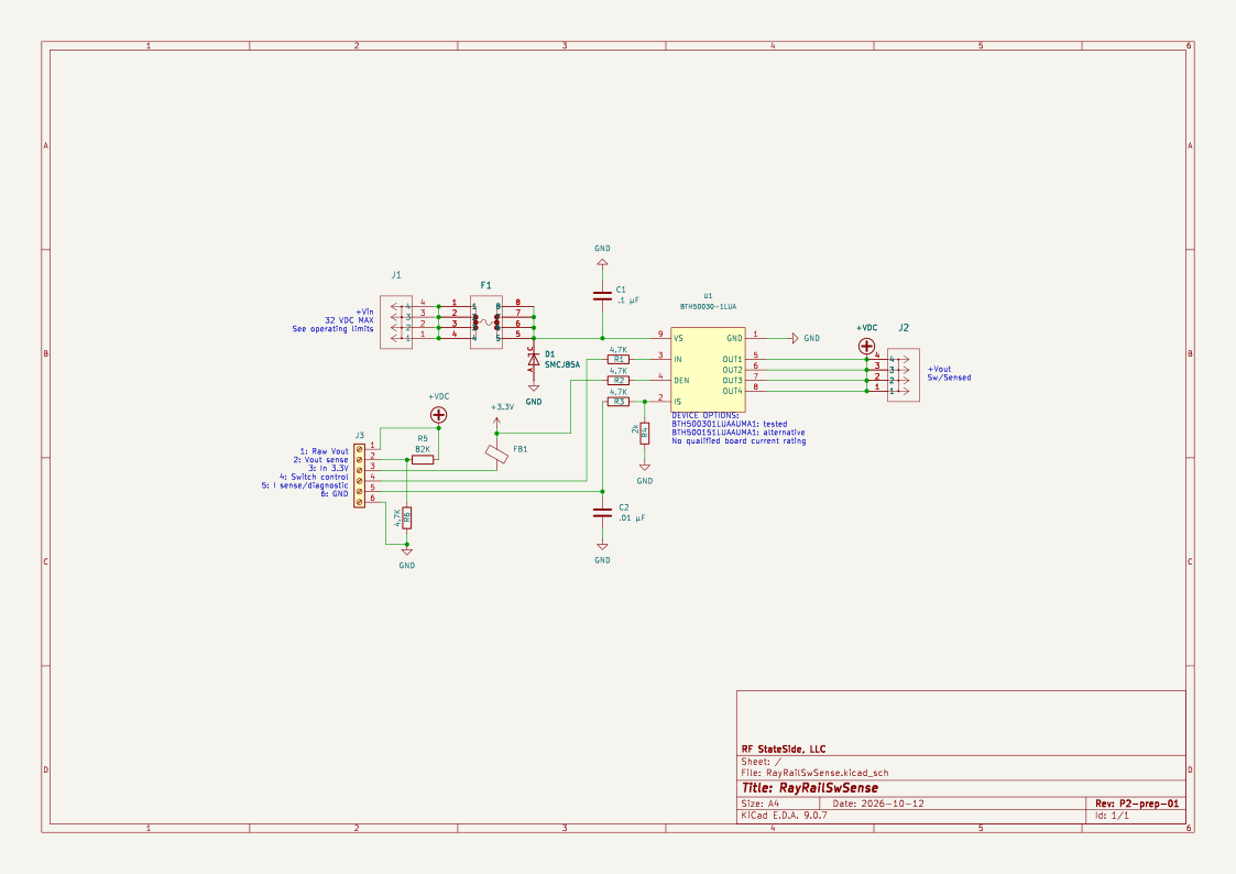
Current P2-prep-01 schematic export. Use it with the integration guide, BOM and known limitations; automated source checks are not physical performance qualification.
Interested in RayRailSwSense?
Study the design and integration requirements, build and test your implementation, modify it, improve it and report findings. Contact Ray for engineering discussion or collaboration.