

RayRigAntSw
Hardware
Through-hole RF relay board for two rigs, three antennas and amplifier/bypass routing. Five 12 V SPDT relays switch the paths; suitable external low-side drivers and controller sequencing are required.
Overview
RayRigAntSw is now an open-hardware Public Engineering Reference — AS-IS under the CERN-OHL-P v2.0 hardware license. The repository supplies editable KiCad sources, a BOM, manufacturing files and integration/assembly documentation for study, independent construction, testing, modification and improvement.
PCBWay fabricated the original boards. RF StateSide assembled and successfully tested them with RaySspaController, which supplied external drivers and sequencing. That historical system integration is distinct from circuitry on this board; parent-controller firmware is not included in the RayRigAntSw release.
The corrected P2-prep-01 manufacturing package has not itself been refabricated or physically tested. Historical testing does not validate the corrected Gerbers. No RF performance guarantee or commercial certification is claimed. The project is Dormant: not currently under active development, available as an engineering reference and open to being revisited.
At a Glance
- • Five 12 V SPDT relays
- • RF amplifier in/out path
- • PTT-1 / PTT-2 routed to external controller
- • Eight-position J8; external low-side drivers
- • 1N5819 flyback diodes + 10 nF coil capacitors
Key Features
Rig & Antenna Routing
- Two rig paths and three antenna paths
- K3/K4 switch amplifier or bypass routing together
- J9/RFlow: amplifier input; J10/RFhigh: amplifier output
- TXRX requires an external low-side driver for two coils
External Controller Responsibilities
- PTT connections pass through to controller sensing
- External controller must arbitrate conflicting PTT requests
- External controller must inhibit RF and sequence switching/amplifier timing
- Board contains no MCU, relay drivers or autonomous interlock
Open Integration
- +12 V supply, GND and four low-side coil-return controls
- Logic levels depend on the chosen external driver
- MCU GPIO pins must not drive relay coils directly
- Historical RaySspaController integration; other controllers require verification
Hardware Overview
K1–K5 are 12 V SPDT relays. The historical procurement reference is Omron G2RL-14-E DC12, not a mandatory substitute specification or proof of the fitted part in every assembly. Each coil has a 1N5819 flyback diode and 10 nF capacitor; this diode/capacitor suppression is not a conventional resistor-capacitor snubber. C6 is the 47 µF supply capacitor.
| Relay(s) | Control return | Switching function |
|---|---|---|
| K1 / K2 | ANT_R1 / ANT_R2 | Select ANT-1 (J3), ANT-2 (J2) or ANT-3 (J1) |
| K5 | RIG_AB | Select RIG-1 (J5) or RIG-2 (J4) |
| K3 / K4 | TXRX (both coils) | Bypass, or selected rig to J9/RFlow (amplifier input) and J10/RFhigh (amplifier output) to selected antenna |
With all coils de-energized, the settled contact route is RIG-1 to ANT-1 through bypass. This describes static contacts, not relay transition timing or a guaranteed safe state. Use the published integration guide for the complete relay truth tables.
J8 — External Controller Interface
| Pin | Signal | Function |
|---|---|---|
| 1 | GND | Supply and control reference |
| 2 | ANT_R1 | K1 low-side coil return |
| 3 | ANT_R2 | K2 low-side coil return |
| 4 | TXRX | K3 and K4 low-side coil returns together |
| 5 | RIG_AB | K5 low-side coil return |
| 6 | PTT-1 | J7 center contact, routed to controller |
| 7 | PTT-2 | J6 center contact, routed to controller |
| 8 | +12 V | Relay supply |
Use suitable external low-side relay drivers, such as a transistor array or MOSFET stage. Do not drive coils directly from MCU GPIO pins. Size drivers and supply wiring for the fitted relay loads, including both TXRX coils and all simultaneously energized coils. Logic voltage and active level depend on the external driver.
PTT jack shells connect to ground. PTT-1/PTT-2 are routed connections, not protected, isolated or logic-processed inputs with guaranteed voltage tolerance. Controller-side sensing, pull-ups, protection and grounding must suit the connected rigs.
System Integration & Switching Responsibilities
RaySspaController provided drivers and sequencing in the historical integration test. Another controller can use the documented interface; its logic and firmware are a separate project.
The external controller must inhibit RF during rig, antenna and path changes, arbitrate conflicting transmit requests, allow relay settling, and sequence amplifier enable/bias around switching. The relay board itself does not enforce transmitter inhibit, safe sequencing, amplifier timing, simultaneous-transmit arbitration or hot-switch prevention.
No RF power rating, frequency range, insertion loss, isolation, return loss, switching lifetime under RF load or hot-switching capability is established by the published reference. Relay contact ratings do not qualify the RF system. Evaluate the complete installation and verify driver/suppression behavior and timing for the actual relays.
Historical Hardware & Corrected Manufacturing Revision
Original PCBWay boards were physically fabricated, assembled and successfully tested with RaySspaController. Their D1–D5 polarity indication was reversed. The diodes were deliberately installed opposite the incorrect markings to achieve correct electrical polarity; this does not mean the tested assemblies had electrically reversed diodes.
Current CAD corrects the historical error. In P2-prep-01, each diode's cathode (banded end, pad 1) connects to +12 V. Historical instructions to reverse the markings do not apply to this corrected set. The retained v2.0 artwork alone cannot identify old versus current fabrication.
The corrected manufacturing files have not been refabricated or physically validated. The release records four inherited clearance findings, two J6 courtyard findings and nine schematic ERC findings; it is not presented as DRC/ERC-clean. Review the engineering audit, known limitations, component fit and fabrication requirements before building. No future development or technical support is promised.
Gallery
Historical board imagery and a current published schematic export. Photos and CAD renderings serve different purposes; none establishes physical acceptance of P2-prep-01.
Assembled Board
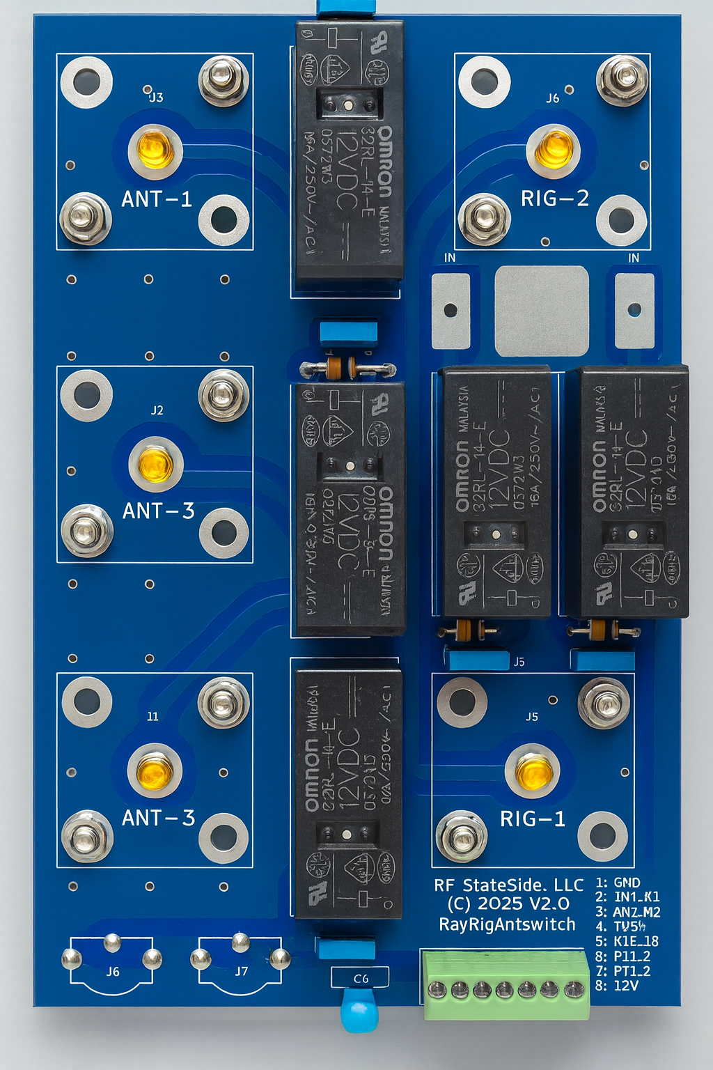
Historical fabricated and assembled RayRigAntSw board with five 12 V SPDT relays. Original RF StateSide hardware photograph; AI was used only for cropping and cleanup. It is historical context, not an assembly authority or a photograph of a validated P2-prep-01 build.
PCB 3D Render
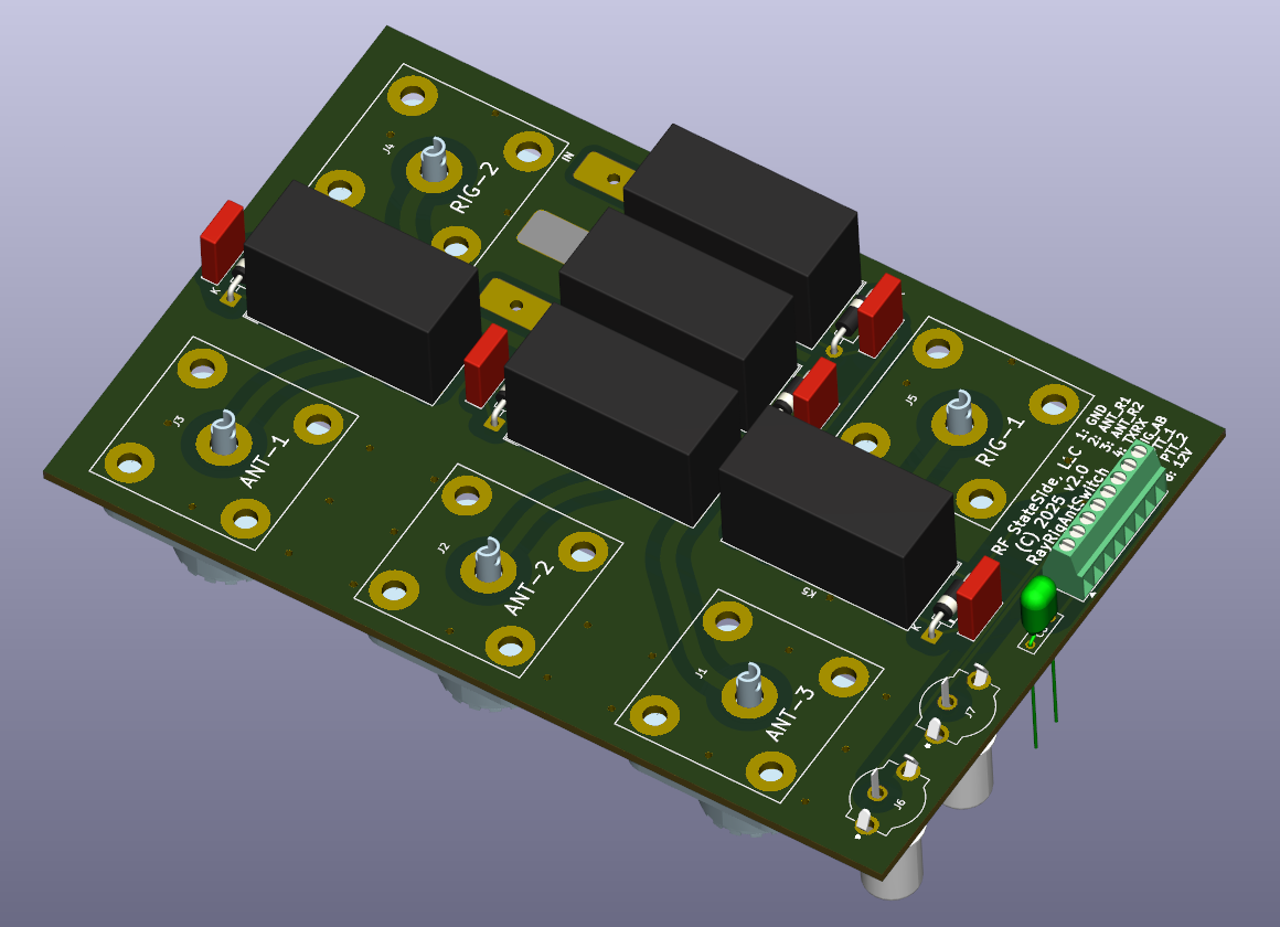
3D render of the RayRigAntSw PCB showing relay placement, RF pads, ANT/RIG routing, and relay-coil diode/capacitor suppression components. This render illustrates the mechanical design, mounting hole positions, and connector layout. This retained historical CAD view is not physical test evidence or the authority for current diode polarity; use the published corrected sources.
Schematic
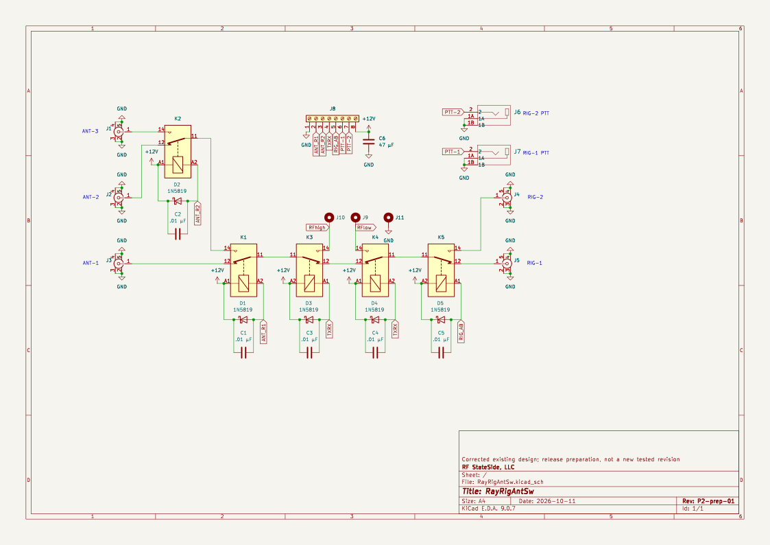
Current P2-prep-01 KiCad schematic export from the public repository, showing the five SPDT relays, 1N5819/10 nF coil suppression and eight-position J8 interface. A CAD rendering, not a physical validation result; no parent-controller firmware is included.
Interested in RayRigAntSw?
Study the published design, build and test your implementation, modify it, improve the documentation, and report findings. Contact Ray for engineering discussion or collaboration.