Resistive Attenuator Calculator
Design simple resistive attenuator pads between equal impedances (e.g., 50 Ω systems). This tool computes resistor values for classic T (tee) and π (pi) pads given a target attenuation in dB and a characteristic impedance Z0.
Current version assumes equal source and load impedances (ZS = ZL = Z0). For impedance-transforming designs, see the Network Matching Tool.
- T-pad: two series arms with a shunt resistor between them.
- π-pad: two shunt resistors with a single series resistor between ports.
All formulas assume resistive networks at the design impedance. Real components have tolerance, power limits, and frequency dependence. For high power, derate generously.
Power handling
- Attenuation (AdB)
- 6.00 dB
- Voltage ratio K = Vin / Vout
- 1.995
- Power ratio Pin / Pout
- 3.981
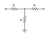
- T (tee) pad – equal impedances
- Two series resistors R1 and R3 with a shunt resistor R2 between them, matched to Z0 on both ports.
- R1 = R3 (series)
- 16.614 Ω
- R2 (shunt to ground)
- 66.931 Ω
- Input power Pin
- 10.00 W
- Output power Pout (approx.)
- 2.68 W
- Total pad dissipation
- 7.32 W
- Resistor wattage (with safety margin)
Resistor Value (Ω) Dissipation (W) With margin (W) Suggested rating R1 16.614 0.890 1.335 2 W R2 66.931 5.543 8.314 10 W R3 16.614 0.890 1.335 2 W Power is approximate for sinusoidal RF at the specified Pin with matched terminations. For very high power or pulsed operation, add additional margin.
For higher power builds, consider using parallel resistors to reduce dissipation per element and improve thermal handling.